Our research explores the fundamental physics of semiconductors at their ultimate thickness limits, focusing on how reduced screening governs carrier dynamics and exciton behavior. We also investigate transport mechanisms in scaled systems to reveal how percolation determines amorphous device beyond conventional electrostatic and quantum limitations.
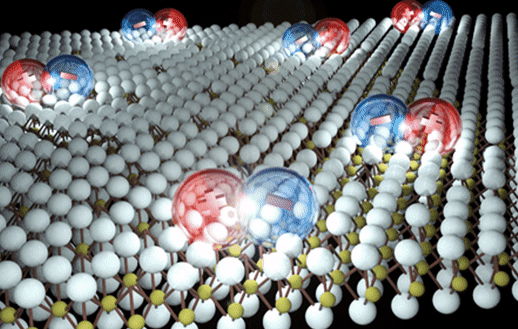
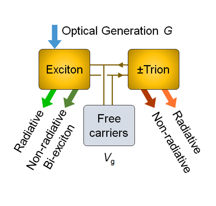
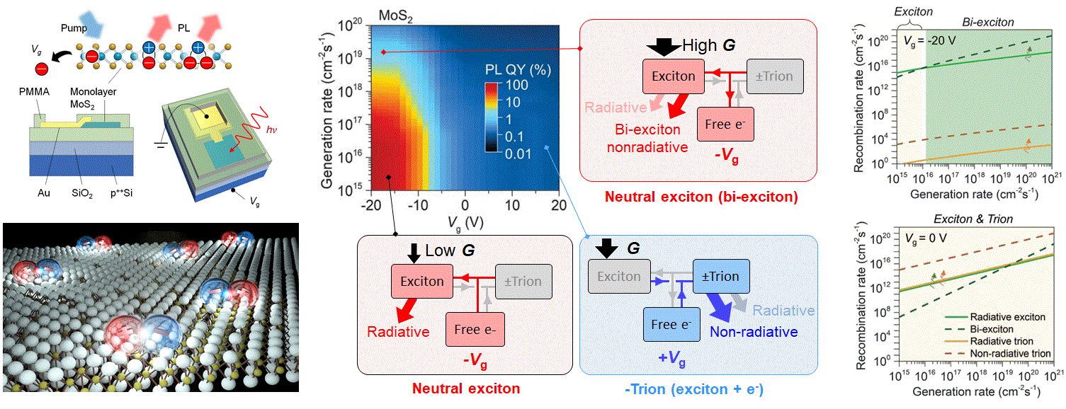
Atomic-thin semiconductors exhibit unique physics because reducing thickness also reduces the screening effect. This leads to strong many-body interactions where carriers become bound as room-temperature excitons. Using monolayer platforms, we were the first to identify the excitonic nature in 2D by analyzing the excitonic recombination process. We demonstrated that these systems achieve near-unity photoluminescence quantum yields through electrostatic doping, even with native defects due to strongly bound excitons. Based on our findings, comprehensive recombination models across various TMDCs were established. Python code for these quasiparticle recombination models is available here.
We also identify a unique dimensional scaling effect in amorphous semiconductors with thickness approaching 2D limits, where reducing channel thickness, width, or length constrains conductive pathways and modulates the percolation threshold. These geometric constraints directly drive threshold voltage shifts, a mechanism observed across different percolative oxide transistors. The findings establish that charge transport in scaled amorphous electronics is governed by geometry-driven percolation transport rather than conventional electrostatics or quantum confinement, presenting key insights for an important class of semiconductors regarding device designs.
Our research explores emerging semiconductors and fundamental atomic-scale properties to develop advanced processing techniques for monolithic 3D integration and back-end-of-line applications. We innovate electronics across fields and bridge academic discovery with industrial manufacturability through collaborations with Taiwanese companies.
My research focuses on the exploration and engineering of emerging semiconductors, including 2D materials, oxide semiconductors, and many others. By investigating fundamental material properties at the atomic scale, we develop advanced processing techniques to enable high-performance monolithic 3D integration and back-end-of-line applications. We aim to bridge the gap between academic discovery and industrial manufacturability. Our work is deeply integrated with the industrial landscape in Taiwan, featuring close collaborations with TSMC and MediaTek to develop next-generation circuits, such as CFETs and beyond.
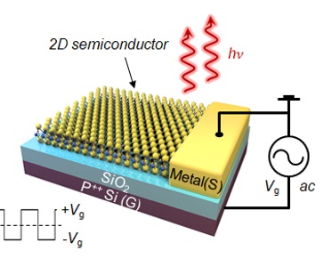
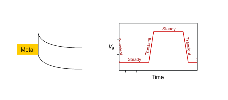
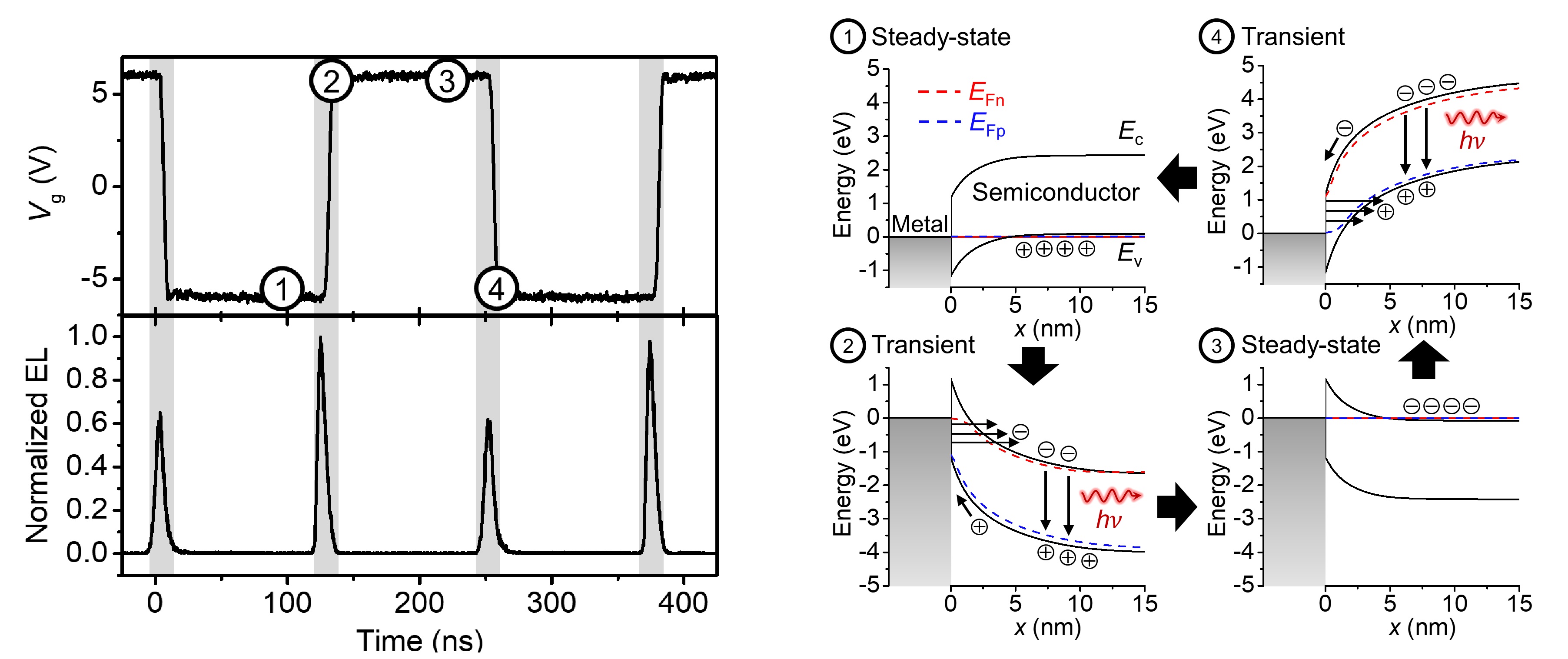
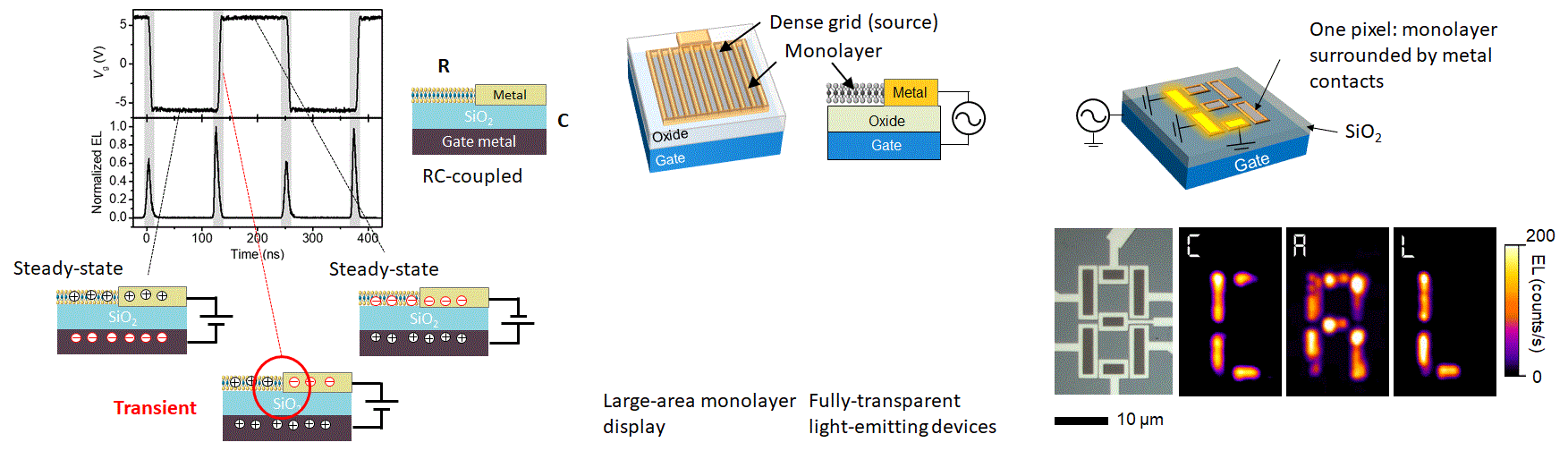
We are also driven by the electronic innovation to bypass conventional physical limitations. I developed a transient-mode AC carrier injection scheme to address the injection inefficiency inherent in Schottky contacts, which enables efficient carrier injection and electroluminescence across various material systems, including 2D, III-V, QDs, etc. Our innovation extends to the forefront of functional integration and advanced packaging, such as memristor-based RF switches integrated on flexible interposers for 3D packaging in 6G communications. We have also pioneered developments in printable memories and resonance-enhanced optoelectronic sensors. Furthermore, we collaborate with industry partners to integrate AI-driven multitask learning algorithms into wearable systems for real-time physiological and biochemical monitoring. Our ultimate goal is to provide a viable pathway for integrating advanced semiconductors into the next generation of versatile electronics.