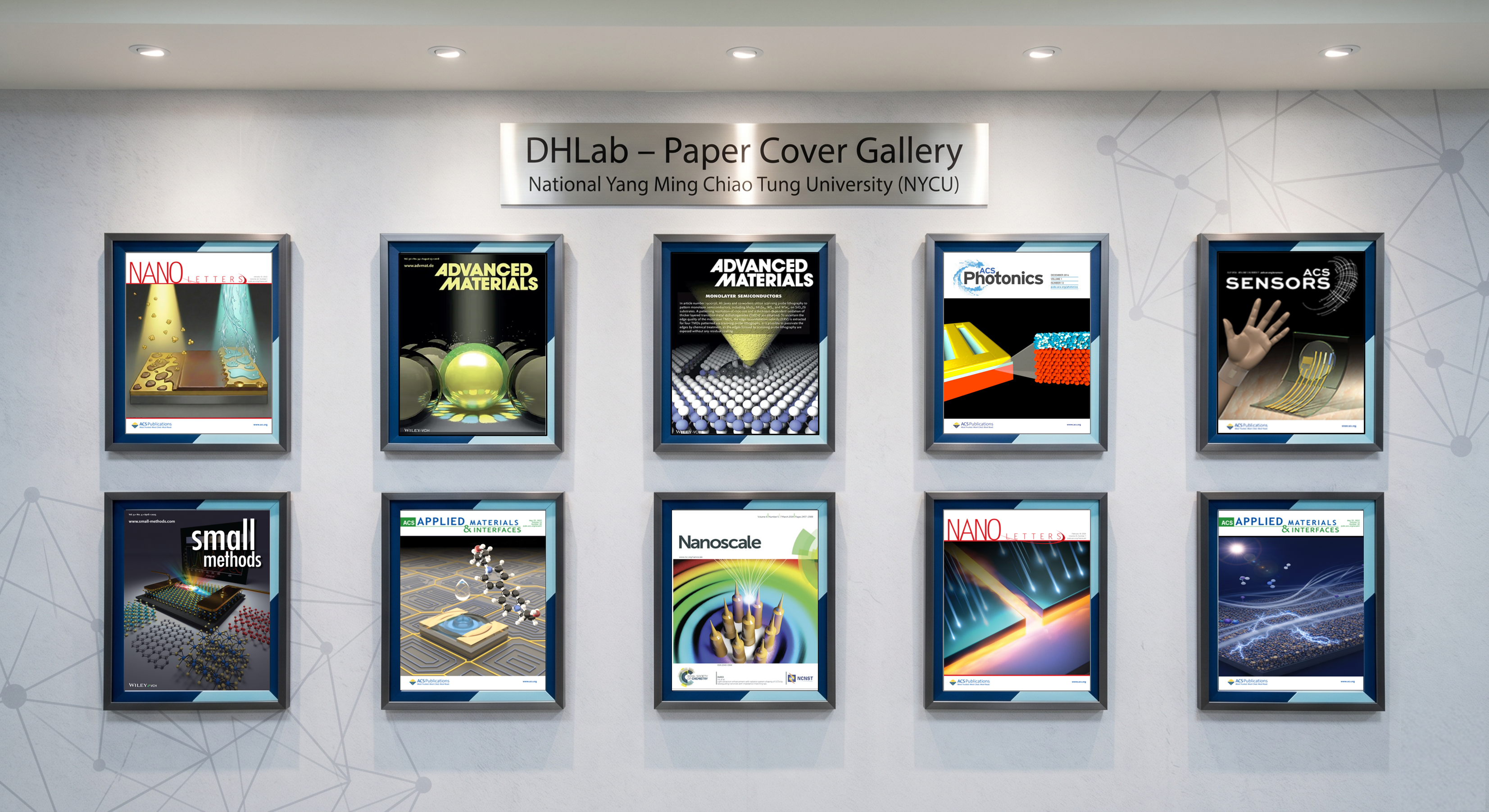
Reversible Thickness Engineering in Amorphous In2O3 Transistors★ Featured on Cover
Nano Letters, 2026.
Dimensional Scaling Effect in Percolative Oxide Semiconductor Transistors
ACS Nano, 2026.
Suppression of Hysteresis in Ultrathin Tellurium Transistors
npj 2D Materials and Applications, 2026.
Origin of Threshold Voltage Instabilities in Indium Oxide Transistors ★ Featured on Cover
ACS Applied Materials & Interfaces, 2026.
Enhanced Crystallinity of P‐Type 2D Tellurium Thin Films by Pulsed Laser Annealing Process and Its Applications on High‐Performance Photodetectors and High‐Sensitivity Gas Sensors
Advanced Functional Materials, e16546, 2025.
Electronic Impact of High-Energy Metal Deposition on Ultrathin Oxide Semiconductors ★ Featured on Cover
Nano Letters, 2025.
HfO2 Memristor-Based Flexible Radio-Frequency Switches
ACS Nano, 19, 704−711, 2025.
A PSPI/PSEP/PSPI Nanocomposite Polymer Interposer Technology for Wireless Edge-AI Microsystem Integration
International Conference on Solid-State Sensors, Actuators and Microsystems (Transducers), 2025.
Homo-Channel WSe2 n/pFETs with High Performance and On/Off Ratio Using Tunable Doping
Symposium on VLSI Technology and Circuits, 2025.
Deep‐UV silicon polaritonic metasurfaces for enhancing biomolecule autofluorescence and two‐dimensional material double‐resonance raman scattering
Advanced Functional Materials, 35 (14), 2025.
Electrical Control of Electroluminescence in 2D Semiconductor Light Emitting Device through Synchronous Injection of Electrons and Holes
Advanced Materials Technologies, 10 (7), 2025.
Improving the thermal stability of indium oxide n-type field-effect transistors
ACS Applied Materials & Interfaces, 17 (3), 5078-5085, 2025.
Breaking the Trade-Off Between Mobility and On–Off Ratio in Oxide Transistors
Adv. Mater., 2413212, 2024.
Emerging 2D Materials and van der Waals Heterostructures for Advanced NIR, SWIR, and MWIR Emitters★ Featured on Cover
Small Methods, 2401550, 2024.
Suppressing threshold voltage drift in sub-2 nm In2O3 transistors with improved thermal stability
IEEE Electron Device Letters, 45, 60, 2024.
Tailoring Electronic Properties of Colloidal Quantum Dots for Efficient Optoelectronics
Advanced Photonics Research, 5 (4), 2300216, 2024.
Wide-range and area-selective threshold voltage tunability in ultrathin indium oxide transistors Highlighted in media
Nature Communications, 14, 5243, 2023.
Reversible charge transfer doping in atomically-thin In2O3 by viologens ★ Featured on Cover
ACS Applied Materials & Interfaces, 16, 5302, 2023.
Multitask Learning for Automated Sleep Staging and Wearable Technology Integration
Advanced Intelligent Systems, 2300270, 2023.
Toward Perfect Surfaces of Transition Metal Dichalcogenides with Ion Bombardment and Annealing Treatment
ACS Appl. Mater. Interfaces, 15, 16153-16161, 2023.
Bright and Efficient Light-Emitting Devices Based on Two-Dimensional Transition Metal Dichalcogenides
Advanced Materials, 2208054, 2023.
Economical Silicon Nanowire Growth via Cooling Controlled Solid–Liquid–Solid Mechanism
Advanced Materials Interfaces, 2202247, 2023.
The Impact of Hot Carrier Injection-Induced Device Degradation for Lower-Power FinFETs
Journal of Electronic Materials, 52 (2), 1391-1399, 2023.
Superacid Treatment on Transition Metal Dichalcogenides
Nano Express, 3, 034002, 2022.
Bright Mid-Wave Infrared Resonant Cavity Light-Emitting Diodes Based on Black Phosphorus
Nano Letters, 22, 1294-1301, 2022.
Defect Inspection Techniques in SiC
Nanoscale Research Letters, 17 (1), 1-17, 2022.
Infrared Photodetectors Based on 2D Materials and Nanophotonics
Advanced Functional Materials, 32, 2111970, 2022.
Study of InGaZnO Thin Film Transistors With Dual Treatment of Pre-Oxidation ZrO2 High-κ Dielectric and Post-Oxidation InGaZnO Channel by Neutral Beam System
Journal of Nanoelectronics and Optoelectronics, 2022.
Recent Advances in Two-Dimensional Quantum Dots and Their Applications
Nanomaterials, 6, 1549, 2021.
Actively variable spectrum optoelectronics with black phosphorus
Nature, 596, 232–237, 2021.
Shape-controlled single-crystal growth of InP at low temperatures down to 220 °C
Proceedings of the National Academy of Sciences (PNAS), 117 (2) 902-906, 2020.
Evaporated tellurium thin films for p-type field-effect transistors and circuits Highlighted in News & Views
Nature Nanotechnology, 15, 53–58, 2020.
Deterministic Assembly of Arrays of Lithographically Defined WS2 and MoS2 Monolayer Features Directly From Multilayer Sources...
Journal of Micro and Nano-Manufacturing, 7(4), 041006, 2020.
Centimeter-Scale and Visible Wavelength Monolayer Light-Emitting Devices
Advanced Functional Materials, 30 (6), 1907941, 2020.
Multiplexed Electroluminescent Device for Emission from Long-Wave Infrared to Ultraviolet Wavelength
Nature Electronics, 3, 612–621, 2020.
Neutral Exciton Diffusion in Monolayer MoS2
ACS Nano, 14, 13433–13440, 2020.
Evaporated SexTe1-x Thin Films with Tunable Bandgaps for Short-Wave Infrared Photodetectors
Advanced Materials, 32, 2001329, 2020.
Substrate-Dependent Exciton Diffusion and Annihilation in Chemically Treated MoS2 and WS2
The Journal of Physical Chemistry C, 2020.
Electrical Suppression of Non-Radiative Recombination Pathways by Electrostatic Doping in Monolayer Semiconductors Highlighted in media
Science, 364, 468–471, 2019.
- "You Don’t Have to Be Perfect for TMDCs to Shine Bright", DOE News
- "Electrostatic doping improves 2D semiconductor performance", Chemistry World
Scanning Probe Lithography Patterning of Monolayer Semiconductors and Its Application for Quantifying Edge Recombination
Advanced Materials, 1900136, 2019.
Optical and electrical properties of two-dimensional palladium diselenide
Applied Physics Letters, 114, 253102, 2019.
Bright electroluminescence in ambient conditions from WSe2 p-n diodes using pulsed injection
Applied Physics Letters, 115, 011103, 2019.
Increasing photoluminescence quantum yield by nanophotonic design of quantum-confined halide perovskite nanowire arrays
Nano Letters, 19, 2850-2857, 2019.
Dip Coating Passivation of Crystalline Silicon by Lewis Acids
ACS Nano, 13, 3723−3729, 2019.
Synthetic WSe2 monolayers with high photoluminescence quantum yield
Science Advances, 5, eaau4728, 2019.
Large-Area and Bright Pulsed Electroluminescence in Monolayer Semiconductors Highlighted in media
Nature Communications, 9, 1129, 2018.
- "Atomically thin light-emitting device opens the possibility for 'invisible' displays", Science Daily / Physics.org
- "'Invisible' display: Cal researchers design atomically-thin, light-emitting device", UPI.com
- "Atoms-Thick Light Emitting Device Promises the Advent of Transparent Displays", Berkeley News
Resonance-Enhanced Absorption in Hollow Nanoshell Spheres with Omnidirectional Detection, High Responsivity and Speed ★ Featured on Cover
Advanced Materials, 1801972, 2018.
Self-Powered Nanodevices for Fast UV Detection and Energy Harvesting using Core-Shell Nanowire Geometry
Nano Energy, 51, 294-299, 2018.
360° Omnidirectional, Printable and Transparent UV Photodetectors for Flexible Electronics
npj Flexible Electronics, 2, 19, 2018.
A Nanostructuring Method to Decouple Electrical and Thermal Transport through the Formation of Electrically Triggered Conductive Nanofilaments
Advanced Materials, 30, 1870243, 2018.
Highly reliable superhydrophobic protection for organic field-effect transistors by fluoroalkylsilane-coated TiO2 nanoparticles
ACS Nano, 12, 11062-11069, 2018.
Extremely reduced dielectric confinement in two-dimensional hybrid perovskites with large polar organics
Communications Physics, 1, 80, 2018.
Methylxanthine drug monitoring with wearable sweat sensors
Advanced Materials, 30, 1707442, 2018.
Highly Stable Near-Unity Photoluminescence Yield in Monolayer MoS2 by Fluoropolymer Encapsulation and Superacid Treatment
ACS Nano, 11, 5179-5185, 2017.
Strain-engineered growth of two-dimensional materials
Nature Communications, 8, 608, 2017.
Measuring the Edge Recombination Velocity of Monolayer Semiconductors
Nano Letters, 17, 5356–5360, 2017.
Improved photoswitching response times of MoS2 field-effect transistors by stacking p-type copper phthalocyanine layer
Appl. Phys. Lett., 109, 183502, 2016.
High Luminescence Efficiency in MoS2 Grown by Chemical Vapor Deposition
ACS Nano, 10, 6535–6541, 2016.
Increased Optoelectronic Quality and Uniformity of Hydrogenated p-InP Thin Films
Chemistry of Materials, 28, 4602–4607, 2016.
Wearable Microsensor Array for Multiplexed Heavy Metal Monitoring of Body Fluids ★ ACS Editors' Choice & Cover
ACS Sensors, 1, 866–874, 2016.
Recombination Kinetics and Effects of Superacid Treatment in Sulfur- and Selenium-Based Transition Metal Dichalcogenides
Nano Letters, 16, 2786–2791, 2016.
Dual-functional Resistive Random Access Memory based on the Push-Pull Mechanism of Oxygen Ions
Scientific Reports, 6, 23945, 2016.
A Wearable Integrated Sensor Array for Perspiration Analysis Highlighted in media >10
Nature, 529, 509–514, 2016.
Monolithic 3D CMOS using Layered Semiconductors
Adv. Mater., 28, 2547–2554, 2016.
Near-Unity Photoluminescence Quantum Yield in MoS2 Highlighted in media
Science, 350, 1065, 2015.
- "Coming to a monitor near you: a defect-free, molecule-thick film", UC Berkeley News
- "Technology Tackling Climate Change", EE Times
- "Conquering the Monolayer-Defect Problem", Optics and Photonics News
- NSF & DOE Office of Science front page
Surface Effect in Metal Oxide-Based Nanoscale Devices Invited Review Paper
Nanoscale, 7, 19874, 2015.
Engineering Light Outcoupling in 2D Materials
Nano Letters, 15, 1356, 2015.
Inkjet-Printed Transparent Nanowire Thin Film Features for UV Photodetectors
RSC Adv., 5, 70707-70712, 2015.
MoS2 Heterojunctions by Thickness Modulation
Scientific Reports, 5, 10990, 2015.
Shape-Dependent Light Harvesting of 3-D Gold Nanocrystals on Bulk Heterojunction Solar Cells
J. Phys. Chem. A, 119, 7554-7564, 2015.
A Fully Transparent Resistive Memory for Extremely Harsh Environments
Scientific Reports, 5, 15087, 2015.
Dual-Gated MoS2/WSe2 van der Waals Tunnel Diodes and Transistors
ACS Nano, 9, 2071, 2015.
Harsh Photovoltaics using InGaN/GaN Multiple Quantum Well Schemes
Nano Energy, 11, 104-109, 2015.
Paper Memory by All-Printing Technology Highlighted Paper
Digest of Symposium on VLSI Technology, 978-1-4799-3332, 2014.
- "Memory Cells Built on Paper" IEEE SPECTRUM / Communications of ACM
- "Fine prints and gigabits of data: on paper" EE Times Europe
All-Printed Paper Memory Top 20 Most Read
ACS Nano, 8, 7613–7619, 2014.
- "Researchers Print Electronic Memory On Paper" Chemical & Engineering News (C&EN)
- "Foldable PC Memory 3D Printed on Normal Paper," SOFTPEDIA
Photon Management in Nanostructured Solar Cells Invited Review
J. Mater. Chem. C. 2, 3144-3171, 2014.
Low-resistivity C54-TiSi2 as a sidewall-confinement nanoscale electrode for three-dimensional vertical resistive memory
Appl. Phys. Lett., 105, 182101, 2014.
A Broadband and Omnidirectional Light-Harvesting Scheme Employing Nanospheres on Si Solar Cells
Nano Energy, 6, 36-43, 2014.
See-Through Ga2O3 Solar-Blind Photodetectors for Use in Harsh Environments
IEEE J. Select. Topics Quantum Elect., 6, 3802006, 2014.
Concurrent Improvement in Photogain and Recovery Time of a Single Metal Oxide Nanowire through Enhancing Surface Band Bending via Incorporating Nanoscale Heterojunction
ACS Photonics, 1, 354-359, 2014.
[Resistive memory for harsh electronics: Immunity to surface effect and high corrosion resistance via surface modification]
Scientific Reports, 4, 4402, 2014.
Trilayered MoS2 Metal-Semiconductor-Metal Photodetectors: Photogain and Radiation Resistance
IEEE J. Select. Topics Quantum Elect., 20, 3800206, 2014.
Few Layer MoS2 with Broadband High Photogain and Fast Optical Switching for Use in Harsh Environments
ACS Nano, 7, 3905, 2013.
Light Extraction Enhancement with Radiation Pattern Shaping of Light Emitting Diodes by Waveguiding Syringe-Like Nanorods with Optical Impedance-Matching Tapered Tips ★ Featured on Cover
Nanoscale, 6, 2624-2628, 2013.
An Efficient Light Extraction Scheme for GaN-Based Light-Emitting Diodes Employing a Hierarchical Structure Consisting of p-GaN Microdomes and SiO2 Nanorods
Appl. Phys. Lett., 103, 161104, 2013.
An energy-harvesting scheme employing CuGaSe2 quantum dot-modified ZnO buffer layers for drastic conversion efficiency enhancement in inorganic–organic hybrid solar cells ★ Featured on Cover
Nanoscale, 5, 6189, 2013.
Solar-blind Photodetectors for Harsh Electronics
Scientific Reports, 4, 2628, 2013.
Ultrasound thermal mapping based on a hybrid method combining cross-correlation and zero-crossing tracking
J. Acoust. Soc. Am., 134, 1530, 2013.
Probing Surface Band Bending of Surface-Engineered Metal Oxide Nanowires
ACS Nano, 6, 9366, 2012.
Critical Capillary Absorption of Current-Melted Silver Nanodroplets into Multiwalled Carbon Nanotubes
Small, 8, 2158, 2012.
Hierarchical Structures Consisting of SiO2 Nanorods and p-GaN Microdomes for Efficiently Harvesting Solar Energy...
Nanoscale, 4, 7346, 2012.
A Supersensitive, Ultrafast, and Broadband Light-Harvesting Scheme Employing Carbon Nanotube/TiO2 Core-Shell Nanowire Geometry
ACS Nano, 6, 6687, 2012.
4H-SiC Metal-Semiconductor-Metal Ultraviolet Photodetectors in Operation of 450°C
IEEE Electron Dev. Lett., 33, 1586, 2012.
Temperature Mapping Technique Based on Ultrasound Signal Analysis
Phys. Med. Biol., 37, S153, 2011.
Direct-current nanogenerator based on ZnO nanotube arrays
Phys. Status Solidi, 5, 77, 2011.
Enhanced Recovery Speed of Nanostructured ZnO Photodetectors Using Nanobelt Networks
IEEE J. Select. Topics Quantum Elect., 18, 1807, 2011.
Single ZnO Micro-/Nanowire Photodetector by Piezo-phototronic Effect
ACS Nano, 4, 6285, 2010.
Resonance frequency shift of a carbon nanotube with a silver nanoparticle adsorbed at various positions
Appl. Phys. Lett., 97, 133105, 2010.
Photoconductive enhancement of single ZnO nanowire through localized Schottky effects
Optics Express, 18, 14836, 2010.
Single-InN-Nanowire Nanogenerator with Upto 1 V Output Voltage
Advanced Materials, 22, 4008–4013, 2010.
Strain promoted conductivity of doped carbon nanotubes
Appl. Phys. Lett., 93, 223111, 2008.
Gas sensing improvement of carbon nanotubes by NH4OH–flash treatment: a nondestructive purification technique
J. Mater. Chem., 17, 3581, 2007.
Nondipolar liquid migration on carbon nanotube films at low field
Appl. Phys. Lett., 89, 044109, 2006.
Segmentation of single-walled carbon nanotubes by camera flash
Appl. Phys. Lett., 88, 093113, 2006.
Photocurrent amplification at carbon nanotube-metal contacts
Advanced Materials, 18, 98- 103, 2006.